PC_Tips_2022

PC_Tips_2022

See also later "part2" (started 20220705U) http://confocal.jhu.edu/mctips/pc_tips_2022_part2

See also earlier PC_Tips_2021  http://confocal.jhu.edu/mctips/pc_tips_2021 

One of the points I made in PC_Tips_2021 is the concept of Distributed Computing Network ("DCN") - that is, some data processing and/or analysis "jobs" can be distributed over many (fast) PC's on a local area network. This can have advantages (sometimes) compared to conventional :Cloud Computing (ex: amazon Web Services), or nearby "supercomputers" (TACC Stampeded, JHU/Md MARCC) in that the data can be inside the network Firewall (re: HIPAA compliance).

***

March 3, 2022 [20220304F] looking foward - (i) local workstation [CPU, GPU], (ii) components of newest exascale HPC


MD MILAN-X EPYC CPUs ... top of the line 7773X list price $9609 ... vs ~$11K for "typical" sCMOS such as ORCA-FLASH4.0LT
 
So (round numbers):
 
$9,000 MILAN-X EPYC CPU [server claass, step up from Threadripper Pro … 128 PCIe lanes … PCIe gen 4? gen5?] 
$1,000 PCIe5 motherboard (or more for 1U server rack, which may be preferable)
$2,000 NVidia RTX 4090  (should be PCIe5, 80 teraflops?) (article at bottom, price my guess, release date in 2H 2022) ... ............................................. ....  RTX 3090 Ti (40 Teraflops) launch $1999 on 20220329U - https://www.tomshardware.com/news/nvidia-geforce-rtx-3090-ti-launches-at-1999-dollars 
$3,000 RAM (maybe 512 GB DDR5?) ... more money, more RAM
$3,000 Highpoint NVMe RAID array (currently PCIe4 so 32 GB/sec, say 16 Terabytes [eight of 2TB])
$2,000 dual HD 4K monitors (~30” each)(???)

<$1000 Ethernet 100 Gbe (50 Gbe) per computer ... also expect same per port of network switch.
-----------
$21,000
 

  • EPYC-7773 Milan list price $8,800 (close to my $9K estmate above) ""AMD Launches Milan-X With 3D V-Cache, EPYC 7773X With 768MB L3 Cache for $8,800" https://www.tomshardware.com/news/amd-launches-milan-x-with-3d-v-cache-epyc-7773x-with-768mb-l3-cache-for-dollar8800
  • motherboards -- or BIOS updates if not new boards -- for newest (3/2022 announced, some on sale) CPUs    https://www.tomshardware.com/news/motherboard-makers-enable-support-for-latest-ryzen-cpus 
  • RTX 30x0 cards ... 20220317Thur - EVGA 3080 Ti GPUs available at EVGA (manufacturer) web site for a day, now sold out https://www.tomshardware.com/news/evga-geforce-rtx-3080-ti-in-stock  ... does high end RTX 30x0 becoming available some day(s) - should get better later in 2022.
  • so one EPYC (server class) CPU would be a bit less than half the price of the workstation/”compute server” (assuming $1K motherboard).
  • IF EPYC Milan too expensive, see new AMD Threadripper 5000WX series workstation CPUs (figure "about half" the price of EPYC, i.e. $5000-$6000 vs $9000 EPYC 'server class' CPU of same 64 cires / 128 threads / 128 PCIe lanes):
  • Workstation CPU 20220308U
  • https://www.tomshardware.com/news/amd-details-ryzen-threadripper-pro-5000-wx-series-zen-3-up-to-64-cores
  • AMD Details Ryzen Threadripper Pro 5000 WX-Series, Zen 3 up to 64 Cores
  • by Paul Alcorn published March 8, 2022
  • AMD announced today that the 'Chagall' Threadripper Pro 5000 WX-series processors will be available to OEM and system integrator partners on March 21, 2022. AMD's new 5000 WX-Series models bring higher clock speeds up to 4.5 GHz, the Zen 3 microarchitecture with a 19% IPC improvement, eight channels of DDR4 memory, 128 lanes of PCIe 4.0, and unified (256MB) L3 cache to AMD's workstation lineup that spans from 12 cores up to the halo 64-core 128-thread Threadripper Pro 5995WX model.
  • another option (Threadripper with 3D cache) ... https://www.tomshardware.com/news/amd-ryzen-7-5800x3d-launch-date-and-price ...  AMD Ryzen 7 5800X3D Arrives April 20 (2022) for $449: Report ... Eight cores with 96MB of L3 cache ... dd in the eight cores with 512KB of L2 each and the chip will feature a whopping 100MB cache. Large caches improve memory bandwidth and single-thread performance, just what the doctor ordered for games ... (ZEN3 has been around a couple of years) ... While Zen 4-based processors are still expected to launch sometime in 2022, AMD's executive implied that it has some new Ryzen 5000 offerings in the pipeline that will address market segments that AMD has not properly addressed yet, such as premium and commercial notebooks.
  • New (20220308U story) Mac M1 also impressive, especially "60 core" GPU having similar performance to NVidia RTX 3090 (a lot morecores, but also different architecture), see https://www.tomshardware.com/news/apple-m1-ultra-mac-studio  -- also likely highly pricey. 

 -----------------------------------------------------------------------------------

Match 4, 2022: 

AMD: EPYC 'Milan-X' CPUs Will Be Available This Month (March 2022)
https://www.tomshardware.com/news/amd-epyc-milan-x-to-launch-this-march-2022

**
https://wccftech.com/amd-milan-x-epyc-7003x-cpus-prices-show-20-percent-more-expensive-3x-more-cache/
 
AMD Milan-X EPYC 7003X CPUs Are About 20% More Expensive Than Standard Milan Chips While Offering 3x More Cache
By Hassan Mujtaba
Feb 25, 2022 09:47 EST
 
 
AMD EPYC Milan-X server CPU lineup will consist of four processors. The EPYC 7773X features 64 cores and 128 threads, the EPYC 7573X features 32 cores and 128 threads, the EPYC 7473X features 24 cores and 48 threads while the EPYC 7373X features 16 cores and 32 threads.
 
The flagship AMD EPYC 7773X will rock 64 cores, 128 threads and feature a maximum TDP of 280W. The clock speeds will be maintained at 2.2 GHz base and 3.5 GHz boost while the cache amount will drive up to an insane 768 MB. This includes the standard 256 MB of L3 cache that the chip features so essentially, we are looking at 512 MB coming from the stacked L3 SRAM which means that each Zen 3 CCD will feature 64 MB of L3 cache. That's an insane 3x increase over the existing EPYC Milan CPUs. In terms of pricing, the EPYC 7773X costs $9609 which is 11% more expensive than the $8616 price of the EPYC 7763.
 
The second model is the EPYC 7573X which features 32 cores and 64 threads with a 280W TDP. The base clock is maintained at 2.8 GHz and the boost clock is rated at up to 3.6 GHz. The total cache is 768 MB for this SKU too. Now interestingly, you don't need to have 8 CCDs to reach 32 cores as that can be achieved with a 4 CCD SKU too but considering that you'd need double the amount of stack cache to reach 768 MB, that doesn't look like a very economical option for AMD and hence, even the lower-core count SKUs might be featuring the full 8-CCD chips. The 7573X costs $6107 which is 14% more expensive than the $5312 US pricing of the EPYC 75F3.
 
With that said, we have the EPYC 7473X which is a 24 core and 48 thread variant with a 2.8 GHz base and 3.7 GHz boost clock and a TDP of 240W while the 16 core and 32 thread EPYC 7373X is configured at a 240W TDP with a base clock of 3.05 GHz and 3.8 GHz boost clock and  768 MB of cache. Both chips cost $4290 and $5137, respectively, which makes them 34 & 32 percent more expensive than their Non-X counterparts.
AMD EPYC Milan-X 7003X Server CPU (Preliminary) Specs:
CPU Name Cores / Threads Base Clock Boost Clock LLC (3D SRAM) L3 Cache (V-Cache + L3 Cache) L2 Cache TDP Price (ShopBLT) Price (MSRP)
AMD EPYC 7773X 64 / 128 2.2 GHz 3.500 GHz Yes (64 MB per CCD) 512 + 256 MB 32 MB 280W (cTDP 225W Down / 280W Up) $9609.36 US TBA
AMD EPYC 7763 64 / 128 2.45 GHz 3.500 GHz N/A 256 MB 32 MB 280W (cTDP 225W Down / 280W Up) $8616.41 US $7890 US
AMD EPYC 7573X 32 / 64 2.80 GHz 3.600 GHz Yes (64 MB per CCD) 512 + 256 MB 32 MB 280W (cTDP 225W Down / 280W Up) $6107.88 US TBA
 

GPU

RTX 3090 Ti launched at $1999 on 20220329U - https://www.tomshardware.com/news/nvidia-geforce-rtx-3090-ti-launches-at-1999-dollars 

**
Subject: NVidia RTX 4090 ... 81 Teraflops (FP32) (maybe) ... vs RTX 3090's 36 Teraflop (FP32)
 

https://wccftech.com/nvidia-geforce-rtx-40-ada-lovelace-gpu-ad102-ad103-ad104-ad106-ad107-leak/ 
 
Previously rumored specs have shown us a huge update to the core specs. The NVIDIA AD102 "ADA GPU" appears to have 18432 CUDA Cores. This is almost twice the cores present in Ampere which was already a massive step up from Turing. A 2.2 GHz clock speed would give us 81 TFLOPs of compute performance (FP32). This is more than twice the performance of the existing RTX 3090 which packs 36 TFLOPs of FP32 compute power.
[power] We have also heard that to support such extreme specifications and the massive increase in SM / Core Count on the AD102 GPU, the top NVIDIA GeForce RTX 40 GPUs such as the RTX 4090 or RTX 4090 Ti could feature a TDP of up to 850W. NVIDIA is already investing development around the new PCIe Gen 5 connector that offers up to 600W power input per connector.
In addition to the SM counts, the Ada Lovelace GPUs will also feature increased L2 cache sizes. Starting with the AD102 GPU, the flagship would be outfitted with up to 96 MB of L2 cache, an insane 16x increase over the 6 MB L2 cache featured on GA102.
It is expected to launch in the second half of 2022 but expect supply and pricing to be similar to current cards despite NVIDIA spending billions of dollars to accquire those good good TSMC 5nm wafers.
 
 
NVIDIA GeForce RTX 40 ‘Ada Lovelace’ GPU Configurations Allegedly Leak Out, Over 18,000 Cores For Flagship AD102 GPU
By Hassan Mujtaba
Mar 1, 2022 14:56 EST
 
NVIDIA GeForce RTX 40 'Ada Lovelace' GPU Configurations Leak Out: AD102 With 144 SMs, AD103 With 84 SMs, AD104 With 60 SMs, AD106 With 36 SMs, AD107 With 24 SMs
Recently, NVIDIA got hacked and hackers were able to steal over 1 TB of confidential information which has started leaking out. Some information that has leaked out in the public already includes a bypass for the LHR technology, source code for DLSS technology, & codenames of next-gen GPU architectures. We have seen information regarding Hopper's successor, Blackwell, leak out that will feature at least two Data Center chips but this latest leak is specific to the consumer GPU lineup on the Ada Lovelace GPU architecture.
 
NVIDIA GeForce RTX 40 'Ada Lovelace' GPU Configurations
 
According to the leak, NVIDIA will have at least six GPUs within its Ada Lovelace lineup. These will include AD102, AD103, AD104, AD106, AD107, and AD10B. The first five SKUs will be designed for the desktop and mobility segments and featured in both GeForce RTX 40 and RTX Workstation solutions. The last part is reported by Kopite7kimi to be specific to the next-gen Tegra SOC while the Ampere-based GA10F could go on to power the next-gen Switch handheld console and Tegra Drive solutions.
 
So coming to the leaked SKUs, the top AD102 GPU which is likely going to power the next-gen GeForce RTX 4090, RTX 4080 Ti graphics cards will make use of 144 SMs, a 71% increase over the existing GA102 GPU and house a massive 18,432 CUDA core count. The interesting thing here is that the AD102 GPU is the only SKU that is getting over a 50% increase in SM count & considering what we have heard about the flagship chip, in terms of performance and power consumption, it looks very likely that NVIDIA is going all out with its top chip in the Ada Lovelace family.
 
The AD103 GPU will replace the GA103 GPU which was recently introduced on mobile and feature the same SM count as the GA102 GPU at 84. The AD104, AD106, and AD107 GPUs will feature 60, 36, and 24 SM units, respectively. Besides the AD103 GPU which is a 40% SM increase over GA103, every other GPU gets a 25-20% SM count increase over its predecessor. It's not as significant as the AD102 GPU but considering this is the mainstream segment, we are likely going to get RTX 3080 or similar performance out of an RTX 4060 Ti & RTX 3070 or higher performance out of the standard RTX 4060. The RTX 4050 should be close or on par with an RTX 3060 given the addition of IPC and clock improvements aside from architectural upgrades.
 
In addition to the SM counts, the Ada Lovelace GPUs will also feature increased L2 cache sizes. Starting with the AD102 GPU, the flagship would be outfitted with up to 96 MB of L2 cache, an insane 16x increase over the 6 MB L2 cache featured on GA102. The AD103 GPU will feature 64 MB, AD104 will feature 48 MB while both AD106/AD107 GPUs will feature 32 MB of L2 cache. As for the memory bus, the flagship AD102 GPU will feature a 384-bit bus interface, the AD103 GPU will get a 256-bit bus interface, AD104 will feature a 192-bit bus interface, while the AD106/AD107 GPUs will get a 128-bit bus interface.
 
NVIDIA Ada Lovelace 'GeForce RTX 40' GPU Configurations
GPU Name GPCs / TPCs SMs Per TPC / Total CUDA Cores L2 Cache Memory Bus
AD102 12 / 6 2 / 144 18432 96 MB 384-bit
AD103 7 / 6 2 / 84 10752 64 MB 256-bit
AD104 5 / 6 2 / 60 7680 48 MB 192-bit
AD106 3 / 6 2 / 36 4608 32 MB 128-bit
AD107 3 / 4 2 / 24 3072 32 MB 128-bit
NVIDIA Ada Lovelace & Ampere GPU Comparison
Ada Lovelace GPU SMs CUDA Cores Memory Bus Ampere GPU SMs CUDA Cores Memory Bus SM Increase (% Over Ampere)
AD102 144 18432 384-bit GA102 84 10752 384-bit +71%
AD103 84 10752 256-bit GA103S 60 7680 256-bit +40%
AD104 60 7680 192-bit GA104 48 6144 256-bit +25%
AD106 36 4608 128-bit GA106 30 3840 192-bit +20%
AD107 24 3072 128-bit GA107 20 2560 128-bit +20%
Previously rumored specs have shown us a huge update to the core specs. The NVIDIA AD102 "ADA GPU" appears to have 18432 CUDA Cores. This is almost twice the cores present in Ampere which was already a massive step up from Turing. A 2.2 GHz clock speed would give us 81 TFLOPs of compute performance (FP32). This is more than twice the performance of the existing RTX 3090 which packs 36 TFLOPs of FP32 compute power.
We have also heard that to support such extreme specifications and the massive increase in SM / Core Count on the AD102 GPU, the top NVIDIA GeForce RTX 40 GPUs such as the RTX 4090 or RTX 4090 Ti could feature a TDP of up to 850W.
NVIDIA is already investing development around the new PCIe Gen 5 connector that offers up to 600W power input per connector. The delayed GeForce RTX 3090 Ti is one example where the card is expected to rock at a TGP of 450W and will be the first desktop graphics card to utilize such a connector interface. The next-gen cards are also expected to utilize the same PCIe standard but it looks like the top variant could end up with two Gen 5 connectors to supplement the ~800W power requirement.
Several PSU makers have already started releasing their brand new Gen 5 power supplies which would include the necessary connectors to support the next-gen GPUs but they only feature one primary Gen 5 connector which means that if NVIDIA was to use a second 16-pin port, users will have to use a 2x 8-pin to 1x 16-pin adapter which will ship with most of these PSUs.
Kopite7kimi also hinted at some specification details of the NVIDIA Ada Lovelace chips a while back which you can read more about here and check out the specs in the table provided below:
NVIDIA CUDA GPU (RUMORED) Preliminary:
GPU TU102 GA102 AD102
Architecture Turing Ampere Ada Lovelace
Process TSMC 12nm NFF Samsung 8nm TSMC 5nm
Die Size 754mm2 628mm2 ~600mm2
Graphics Processing Clusters (GPC) 6 7 12
Texture Processing Clusters (TPC) 36 42 72
Streaming Multiprocessors (SM) 72 84 144
CUDA Cores 4608 10752 18432
L2 Cache 6 MB 6 MB 96 MB
Theoretical TFLOPs 16.1 37.6 ~90 TFLOPs?
Memory Type GDDR6 GDDR6X GDDR6X
Memory Bus 384-bit 384-bit 384-bit
Memory Capacity 11 GB (2080 Ti) 24 GB (3090) 24 GB (4090?)
Flagship SKU RTX 2080 Ti RTX 3090 RTX 4090?
TGP 250W 350W 450-850W?
Release Sep. 2018 Sept. 20 2H 2022 (TBC)
The NVIDIA Ada Lovelace GPU family is expected to bring a generational jump similar to Maxwell to Pascal. It is expected to launch in the second half of 2022 but expect supply and pricing to be similar to current cards despite NVIDIA spending billions of dollars to accquire those good good TSMC 5nm wafers.

https://spectrum.ieee.org/intel-s-exascale-supercomputer-chip-is-a-master-class-in-3d-integration
Behind Intel’s HPC Chip that Will Pierce the Exascale Barrier Ponte Vecchio packs in a lot of silicon to power the Aurora supercomputer 
SAMUEL K. MOORE25 FEB 2022
[parts of story below]
On Monday, Intel unveiled new details of the processor that will power the Aurora supercomputer, which is designed to become one of the first U.S.-based high-performance computers (HPCs) to pierce the exaflop barrier—a billion billion high-precision floating-point calculations per second. Intel Fellow Wilfred Gomes told engineers virtually attending the IEEE International Solid State Circuits Conference this week that the processor pushed Intel’s 2D and 3D chiplet integration technologies to the limits.

The processor, called Ponte Vecchio, is a package that combines multiple compute, cache, networking, and memory silicon tiles, or “chiplets.” Each of the tiles in the package is made using different process technologies, in a stark example of a trend called heterogeneous integration.
“Ponte Vecchio started with a vision that we wanted democratize computing and bring petaflops to the mainstream,” said Gomes. Each Ponte Vecchio system is capable of more than 45 trillion 32-bit floating-point operations per second (teraflops). Four such systems fit together with two Sapphire Rapids CPUs in a complete compute system. These will be combined for a total exceeding 54,000 Ponte Vecchios and 18,000 Sapphire Rapids to form Aurora, a machine targeting 2 exaflops.

It’s taken 14 years to go from the first petaflop supercomputers in 2008—capable of one million billion calculations per second—to exaflops today, Gomes pointed out. A 1000-fold increase in performance

***

2022 looks like a great year to purchase new PC hardware to go much faster than 5 years ago (GM arrived ar Ross image core May 2017).

Computer Performance 2017 vs 2022
  Component

2017    and image core improvements (as of 1/2022)


2022                                                                                                                                                                                                 

  Drive speed

Hard disk drive HDD 100 MB/sec = 0.1 GB/sec
SATA-6 solid state drive 600 MB/sec = 0.6 GB/sec
NVMe solid state drive 3,000 MB/sec = 3 GB/sec (PCIe gen3)

* NVMe PCIe (gen3) NVMe array ~16 GB/sec (Highpoint)


Image Core: NVMe PCIe3 arrays, ~3 GB/sec, 4 TB capacity, main acquisition PC's (2 confocals, 1 widefield) & GM's desktop PC.

NVMe PCIe gen 3 single drive   3 GB/sec
NVMe PCIe gen 4 single drive   7 GB/sec
NVMe PCIe gen 5 single drive 13 GB/sec

* NVMe PCIe (gen3) NVMe array ~16 GB/sec (Highpoint)
* NVMe PCIe (gen4) NVMe array ~32 GB/sec (Highpoint)
* NVMe PCIe (gen4) NVMe array ~40 GB/sec  dual PCIe cards (Highpoint)
https://www.amazon.com/HighPoint-Technologies-SSD7540-8-Port-Controller/dp/B08LP2HTX3
future PCIe gen5 array ... ~64 GB/sec


**

20220428H - GRAID dual width PCIe4 RAID NVMe array controller for up to 32 NVMe drives

GRAID SupremeRAID PCIe3 controller (32 NVMe drives)

GRAID Technology 20220501 launch - SupremeRAID SR-1010 holds up to 32 NVMe drives Windows Server 2019 or 2022 or Linux
https://www.graidtech.com/supremeraid-sr-1010  
https://www.gigabyte.com/Article/gigabyte-server-and-graid-supremeraid%E2%84%A2    (this is use of earlier PCIe3 model)

https://www.tomshardware.com/news/gpu-powered-raid-110-gbps-19-million-iops
110 Gbps = 13.75 GBps
22 Gbps = 2.75 GBps
PCIe4 is 32 GBps
The SupremeRAID SR-1010 features a dual-slot design and measures 2.713 x 6.6 inches (height x length). 
PCIe 4.0 interface (takes up 2 PCIe slots). The maximum power consumption of 70W is only 20W higher than its predecessor. The SupremeRAID SR-1010 admits RAID 0, 1, 5, 6, and 10 arrays like the previous model. The card manages up to 32 directly attached NVMe SSDs and supports the most popular Linux distributions and Windows Server 2019 and 2022.
The SupremeRAID SR-1010 will be available starting May 1 through GRAID Technology's authorized resellers and OEM partners. The card's pricing is unknown.

**
20220428Thur some NVMe prices
Samsung 980 Pro NVMe    https://www.amazon.com/SAMSUNG-Internal-Gaming-MZ-V8P2T0B-AM/dp/B08RK2SR23
1TB ... $110
2TB ... $290
Sabrent Rocket 4 Plus NVMe PCIe4   https://www.amazon.com/4TB-SSD-Heatsink-PS5-SB-RKT4P-PSHS-4TB/dp/B09G2P4PYP
1TB ... $160
2TB ... $310
4TB ... $710
32 * 4 TB = 128 TB, $22,720 (for 32 drives, not include SR-1010 or E-ATX motherboard, big power supply etc). 


  Drive capacity

single HDD drive ~10 Teraflops ... RAID array could be big. RAID also good to scale speed (ex.8 drives at 100 MB/sec enables ~800 MB/sec).

In practice, a single fluorescent microscope might acquire 1 Terabyte/year (ex: our confocal microscopes with ~1000 hours use, i.e. 1 GB/hour) ... and we now routinely have users upload their data to their JH OneDrive (each JHU staff and student "gets" 5 Terabytes Microsoft OneDrive capacity each, can get morespace). 

Image Core: NVMe PCIe3 arrays, ~3 GB/sec, 4 TB capacity, main acquisition PC's (2 confocals, 1 widefield) & GM's desktop PC.

File server: 40 TB HDD RAID array (with 10 Gbe Ethernet on backplane, inspiring 10 Gbe network throughout core) - created by John gibas, GM's predecessor as image core manager.

Capacitry is not really a problem - more of 'speed, within budget" is good. 
 

motherboard

and case

E-ATX

and big case

Image core: all ATX or smaller.

E-ATX ... figure $1000 for PCIe gen5 motherboard

and big case

  Power supply

?

Image core: mostly whatever was in PC chassis on purchase.

1000 Watt is likely going to be needed
  CPU

various Intel (Zeon etc) or AMD (ZEN2) --> AMD ZEN3 (newer PCs) ... in 2022 ZEN4, ZEN5 in play and Intel now offers "Alder Lake" CPUs across very broad feature : prices range.

Intel launched new CPUs late 2021 and at CES 1/2022. 

AMD launch(ing) ZEN4 CPUs "winter/spring 2022", PCIe5 (again, lots of PCIe lanes addressed directly by CPU, no "bridge" chip).

The new 2022 CPUs are matched to new faster RAM.("memory lanes"). 

xx

PCIe lanes controlled by CPU vs bridge chip

GM has not seen clear documentation on whether CPU "direct" lanes access is better than through "bridge" chip. PCIe lanes and "memory lanes" both important. Historically, Intel consumer CPUs max'd out at 16 PCIe lanes, whereas AMD 64 PCIe3 lanes (Threadripper) or 128 lanes (Threadripper Pro, EPYC server class CPUs).

20220127H:: Chat with the light microscope facility manager at Carneigie Institute of Embryology (which is on the JHU Homewood campus - my apology for not getting their full name at a Nikon SoRa demo) they told me that for CPUs require a PCIe bridge chip, that the key to performance is how many lanes are used for each of CPU - Bridge and Bridge - PCIe lanes and that this depends on the motherboard archietecture. For example, if the CPU - bridge is x4 lanes and bridge - PCIe lanes is x4, then throughput is going to be throttled by the x4 bottleneck, even if the PCIe slots are x16. 

Upshot: regardless of CPU (Intel vs AMD) that your PCIe performancas depends on whether you purchase the right motherboard.

Intel's new CPUs - pay as you go feature upgrades

GM note: article avoids mentioning Microsoft Windows (Win10, 11, Server).

  GM: nice idea in that few customers (at least consumers) would have >2 TB RAM on their new PC, so why charge a premium to all customers if that feature can be enabled by a software "patch" later. ... On the other hand, any feature upgradable by software can probably be hacked.

https://www.tomshardware.com/news/intel-software-defined-cpu-support-coming-to-linux-518

Intel's Pay-As-You-Go CPU Feature Gets Launch Window

By Anton Shilov - Feb 9, 2022

Intel's software-upgradeable CPUs to be supported by Linux 5.18 this Spring.

Intel's mysterious Software Defined Silicon (SDSi) mechanism for adding features to Xeon CPUs will be officially supported in Linux 5.18, the next major release of the operating system. SDSi allows users to add features to their CPU after they've already purchased it. Formal SDSi support means that the technology is coming to Intel's Xeon processors that will be released rather shortly, implying Sapphire Rapids will be the first CPUs with SDSi.  

Intel Software Defined Silicon (SDSi) is a mechanism for activating additional silicon features in already produced and deployed server CPUs using the software. While formal support for the functionality is coming to Linux 5.18 and is set to be available this spring, Intel hasn't disclosed what exactly it plans to enable using its pay-as-you-go CPU upgrade model. We don't know how it works and what it enables, but we can make some educated guesses. 

very generation of Intel Xeon CPUs adds multiple capabilities to make Intel's server platform more versatile. For example, in addition to microarchitectural improvements and new instructions, Intel's Xeon Scalable CPUs (of various generations) added support for up to 4.5TB of memory per socket, network function virtualization, Speed Select technology, and large SGX enclave size, just to name a few. In addition, there are optimized models for search, virtual machine density, infrastructure as a service (IaaS), software as a service (SaaS), liquid cooling, media processing, and so on. With its 4th Generation Xeon Scalable 'Sapphire Rapids' CPUs, Intel plans to add even more features specialized for particular use cases. You can see an example of the SKU stack above, and it includes all types of different Xeon models:

L- Large DDR Memory Support (up to 4.5TB)
M- Medium DDR Memory Support (up to 2TB)
N- Networking/Network Function Virtualization
S- Search
T- Thermal
V- VM Density Value
Y- Intel Speed Select Technology

But virtually none of Intel's customers need all the supported features, which is why Intel has to offer specialized models. There are 57 SKUs in the Xeon Scalable 3rd-Gen lineup, for example. But from a silicon point of view, all of Intel's Xeon Scalable CPUs are essentially the same in terms of the number of cores and clocks/TDP, with various functionalities merely disabled to create different models. 

Intel certainly earns premium by offering workload optimized SKUs, but disabling certain features from certain models, then marking them appropriately and shipping them separately from other SKUs (shipped to the same client) is expensive — it can be tens of millions of dollars per year (or even more) of added logistical costs, not to mention the confusion added to the expansive product stack. 

But what if Intel only offers base models of its Xeon Scalable CPUs and then allows customers to buy the extra features they need and enable them by using a software update? This is what SDSi enables Intel to do. Other use cases include literal upgrades of certain features as they become needed and/or repurposing existing machines. For example, if a data center needs to reconfigure CPUs in terms of clocks and TDPs, it would be able to buy that capability without changing servers or CPUs. 

Advertisement

Intel yet has to disclose all the peculiarities of SDSi and its exact plans about the mechanism, but at this point, we are pretty certain that the technology will show up soon.

CPU packaging with on package HBM2E memory (likely server class format CPU) ... hmmm - 2E obsoleted by 3 specification (see bottom of table below)

Intel marketign claim big speed up CPU and some RAM "on package"

20220218Fri from TomsHardware - A. Shilov post (20220217Thur).

Reminder: "Marketing, marketing,, marketing, all is marketing saith the preacher" (re: Ecclesiastes). AMD Milan-X is (2022 H2) ZEN4 CPU family.

Not currently a product -- end of article: "Intel will ship its Xeon Scalable 'Sapphire Rapids' processors with on-package HBM2E memory in the second half of the year."

Near bottom of story: "The addition of on-package 64GB HBM2E memory increases bandwidth available to Intel Xeon 'Sapphire Rapids' processor to approximately 1.22 TB/s, or by four times when compared to a standard Xeon 'Sapphire Rapids' CPU with eight DDR5-4800 channels. This kind of uplift is very significant for memory bandwidth dependent workloads, such as computational fluid dynamics. "

https://www.tomshardware.com/news/intel-sapphire-rapids-with-hbm-is-2x-faster-than-amds-milan-x

Intel: Sapphire Rapids with HBM Is 2X Faster than AMD's Milan-X

By Anton Shilov published 20220217

In memory bound workloads.

Intel's fourth Generation Xeon Scalable 'Sapphire Rapids' processors can get a massive performance uplift from on-package HBM2E memory in memory-bound workloads, the company revealed on Thursday. The Sapphire Rapids CPUs with on-package HBM2E are about 2.8 times faster when compared to existing AMD EPYC 'Milan' and Intel Xeon Scalable 'Ice Lake' processors. More importantly, Intel is confident enough to say that its forthcoming part is two times faster than AMD's upcoming EPYC 'Milan-X.' 

"Bringing [HBM2E memory into Xeon package] gives GPU-like memory bandwidth to CPU workloads," said Raja Koduri, the head of Intel's Intel's Accelerated Computing Systems and Graphics Group. "This offers many CPU applications, as much as four times more memory bandwidth. And they do not need to make any code changes to get benefit from this."

To prove its point, Intel took the OpenFOAM computational fluid dynamics (CFD) benchmark (28M_cell_motorbiketest) and ran it on its existing Xeon Scalable 'Ice Lake-SP' CPU, a sample of its regular Xeon Scalable 'Sapphire Rapids' processor, and a pre-production version of its Xeon Scalable 'Sapphire Rapids with HBM' CPU, revealing rather massive advantage that the upcoming CPUs will have over current platforms.  

The difference that on-package HBM2E brings is indeed very significant: while a regular Sapphire Rapids is around 60% faster than an Ice Lake-SP, an HBM2E-equipped Sapphire Rapids brings in a whopping 180% performance boost.

What is perhaps more interesting is that Intel also compared performance of its future processors to an unknown AMD EPYC 'Milan' CPU (which performs just like Intel's Xeon 'Ice Lake', according to Intel and OpenBenchmarking.org) as well as yet-to-be-released EPYC 'Milan-X' processor that carries 256MB of L3 and 512MB of 3D V-Cache. Based on results from Intel, AMD's 3D V-Cache only improves performance by about 30%, which means that even a regular Sapphire Rapids will be faster than this part. By contrast, Intel's Sapphire Rapids with HBM2E will offer more than two times (or 115%) higher performance than Milan-X in OpenFOAM computational fluid dynamics (CFD) benchmark. 

Performance claims like these made by companies must be verified by independent testers (especially given the fact that some other benchmark results show a different picture), but Intel seems to be very optimistic about its Sapphire Rapids processors equipped with HBM2E memory. 

The addition of on-package 64GB HBM2E memory increases bandwidth available to Intel Xeon 'Sapphire Rapids' processor to approximately 1.22 TB/s, or by four times when compared to a standard Xeon 'Sapphire Rapids' CPU with eight DDR5-4800 channels. This kind of uplift is very significant for memory bandwidth dependent workloads, such as computational fluid dynamics. What is even more attractive is that developers do not need to change their code to take advantage of that bandwidth, assuming that the Sapphire Rapids HBM2E system is configured properly and HBM2E memory is operating in the right mode. 

"Computational fluid dynamics is one of the applications that benefits from memory bandwidth performance," explained Koduri. "CFD is routinely used today inside a variety of HPC disciplines and industries significantly reducing product development, time and cost. We tested OpenFOAM, a leading open source HPC workload for CFD on a pre-production Xeon HBM2E system. As you can see it performs significantly faster than our current generation Xeon processor."

Intel will ship its Xeon Scalable 'Sapphire Rapids' processors with on-package HBM2E memory in the second half of the year.

***

part of Nov 15, 2021 story below

https://www.tomshardware.com/news/intels-sapphire-rapids-to-have-64-gigabytes-of-hbm2e-memory

All told, Intel's Sapphire Rapids data center chips come with up to 64GB of HBM2e memory, eight channels of DDR5, PCIe 5.0, and support for Optane memory and CXL 1.1, meaning they have a full roster of connectivity tech to take on AMD's forthcoming Milan-X chips that will come with a different take on boosting memory capacity.

While Intel has gone with HBM2e for Sapphire Rapids, AMD has decided to boost L3 capacity using hybrid bonding technology to provide up to 768MB of L3 cache per chip. Sapphire Rapids will also grapple with AMD's forthcoming Zen 4 96-core Genoa and 128-core Bergamo chips, both fabbed on TSMC's 5nm process. Those chips also support DDR5, PCIe 5.0, and CXL interfaces. 

Computer specifications ... love 'em ... HBM3 mostly for data centers - potentially server rack(s)

https://hothardware.com/news/hbm3-specification-819gbs-bandwidth

by Paul Lilly — Friday, January 28, 2022

HBM3 Specification Leaves HBM2E In The Dust With 819GB/s Of Bandwidth

At long last, there's an official and finalized specification for the next generation of High Bandwidth Memory. JEDEC Solid State Technology Association, the industry group that develops open standards for microelectronics, announced the publication of the HBM3 specification, which nearly doubles the bandwidth of HBM2E. It also increase the maximum package capacity.

So what are we looking at here? The HBM3 specification calls for a doubling (compared to HBM2) of the per-pin data rate to 6.4 gigabits per second (Gb/s), which works out to 819 gigabytes per second (GB/s) per device.
To put those figures into perspective, HBM2 has a per-pin transfer rate of 3.2Gb/s equating to 410GB/s of bandwidth, while HBM2E pushes a little further with a 3.65Gb/s data rate and 460GB/s of bandwidth. So HBM3 effectively doubles the bandwidth of HBM2, and offers around 78 percent more bandwidth than HBM2E.
What paved the way for the massive increase is a doubling of the independent memory channels from eight (HBM2) to 16 (HBM3). And with two pseudo channels per channel, HBM3 virtually supports 32 channels.
Once again, the use of die stacking pushes capacities further. HBM3 supports 4-high, 8-high, and 12-high TSV stacks, and could expand to a 16-high TSV stack design in the future. Accordingly, it supports a wide range of densities from 8Gb to 32Gb per memory layer. That translates to device densities ranging from 4GB (4-high, 8Gb) all the way to 64GB (16-high, 32Gb). Initially, however, JEDEC says first-gen devices will be based on a 16Gb memory layer design.
"With its enhanced performance and reliability attributes, HBM3 will enable new applications requiring tremendous memory bandwidth and capacity," said Barry Wagner, Director of Technical Marketing at NVIDIA and JEDEC HBM Subcommittee Chair.
There's little-to-no chance you'll see HBM3 in NVIDIA's Ada Lovelace or AMD's RDNA 3 solutions for consumers. AMD dabbled with HBM on some of its prior graphics cards for gaming, but GDDR solutions are cheaper to implement. Instead, HBM3 will find its way to the data center.
SK Hynix pretty much said as much last year when it flexed 24GB of HBM3 at 819GB/s, which can transmit 163 Full HD 1080p movies at 5GB each in just one second. SK Hynix at the time indicated the primary destination will be high-performance computer (HPC) clients and machine learning (ML) platforms.


  GPU

NVidia Titan X ~3 teraflops double precision (PCIe gen 3).

Image core:

FISHscope: NVidia RTX 2080 Ti GPU 11GB (cellSens C.I. deconvolution).

Leica SP8 (HP Z640): NVidia M6000 GPU (Maxwell architecture = old, GPU that came with PC, no upgrades due to chassis & motherboard constraints) GPU used by SVI.nl Huygens GPU deconvolution ("HyVolution2" combination of Leica HyD detectors, Huygens).

GM PC: NVIDIA Quadro 2000 (no need for more modern card since not doing GPU deconvolution on this PC).

NVidia RTX 3090 Ti ~20 Teraflop double precision, PCIe gen 4 (Ampere architecture).


near futue: RTX 40x0 series ("Ada Lovelace" architecture [1 generation past Ampere in 30x0 models), 40 (maybe 50) Teraflop by end of 2022, PCIe gen5.

In 2021 NVidia software drivers -- on select modern PCIe4 motherboards - enabled "resiazable BAR" (see PC_Tips_2021) for bigger data transfers between GPU ram and main system RAM. Essentially, now can transfer 'unlimited' (except by GPU ram, since usually more system RAM) data, instead of historic limit of 256 MB memory aperture. This means, for example, a 1 GB Z-series could be moved onto (and results later off of) GPU in one transfer. Same with upcoming PCIe5 -- which is 2x throughput of PCIe4.

Note: I emphasize NVidia over AMD for GPUs because most (maybe all) deconvolution software has been developed to run on NVidia cards, notably SVI.nl Huygens, Microvolution (www.microvolution.com), AutoQuant (part of Media Cybernetics), various microscope vendors (often featuring "A.I"/ deep learning, which play well on NVidia 20x0 and 30x0 GPUs), such as Leica THUNDER/LIGHTNING, Olympus cellSens constrained iterative ("C.I.") deconvolution, Nikon Elements, Zeiss ZEN.

  RAM

  64 GB was "a lot" in 2012 (and pricey).

Image core: several PCs 64 GB ram, one has 256 GB ram. 

  64 GB (PCIe gen4) was ~$600 in mid-2021 when GM purchased a new PC for home (PowerSpec G509 from MicroCenter) so ~$10 / GB. 

2022: PCIe5 will play well with new fast RAM (DDR5, DDR6, on GPU GDDR6).

Some RAM prices

https://www.tomshardware.com/news/ddr5-availability-improving-prices-dropping
32GB dual-channel DDR5-4800, DDR5-5200, DDR5-5600, and DDR5-6000 kits.

                                                                           Dec 2021     Late Jan 2022
Crucial DDR5-4800 CL40                                    $1000              $450 (URL below)
Kingston Fury Beast DDR5-5200 CL40               $1000              $428
G.Skill Trident Z DDR5-5600 CL36                      $1000              $510
G.Skill Trident Z DDR5-6000 CL36                      $3660              $810

Comparison                                                     June 2021   Late Jan 2022
DDR4-3600  (GM's home PC)                               $170             $140
https://www.amazon.com/gp/product/B0884TNHNC purchasedd as 2x32GB price above is per 32GB.

20220127Thur amazon URL and current price ($450 for 32GB stick, as in table above):

https://www.amazon.com/Crucial-4800MHz-Desktop-Memory-CT32G48C40U5/dp/B09HW97JVF
Crucial RAM 32GB DDR5 4800MHz CL40 Desktop Memory CT32G48C40U5
$450

I note that amazon prices are lower for two 16GB ram than one 32GB ram. Advantage of the latter is "more capacity per motherboard slot" (need to check with data sheet and manual of motherboard to make sure PC can support higher capacity RAM ships AND higher total RAM in PC -- also may need higer "tier" (higher price - though may be invislble in academia or big companies) of Windows 10 Enterprise or Windows 2016 Server (which need to be X64 -- no one should be using X32 [x86] in 2022 !!!), see

https://docs.microsoft.com/en-us/windows/win32/memory/memory-limits-for-windows-releases

Limits on memory and address space vary by platform, operating system, and by whether the IMAGE_FILE_LARGE_ADDRESS_AWARE value of the LOADED_IMAGE structure and 4-gigabyte tuning (4GT) are in use. IMAGE_FILE_LARGE_ADDRESS_AWARE is set or cleared by using the /LARGEADDRESSAWARE linker option.

6TB   Windows 10 Enterprise 6TB onX64

6TB   Windows 10 Pro for Workstations on X64 ... 4TB on X86

2TB   Windows 10 Pro on X64 ... weird; 4TB on X86

128GB   Windows 10 Home on X64 ...weird, 4TB on X86

24TB Windows Server 2016 Datacenter or 2016 Standard

4TB   Windows Server 2012 Datacenter or 2012 Standard


HBM3 interface = fast (1/2022)


https://www.tomshardware.com/news/hbm3-spec-reaches-819-gbps-of-bandwidth-and-64gb-of-capacity

HBM3 Spec Reaches 819 GBps of Bandwidth and 64GB of Capacity (High Bandwidth Memory )

By Mark Tyson - January 28, 2022

Huge uplift over HBM2E's max 3.65 Gbps, 460 GBps.

The evolution of High Bandwidth Memory (HBM) continues with the JEDEC Solid State Technology Association finalizing and publishing the HBM3 specification today, with the standout features including up to 819 GBps of bandwidth coupled with up to 16-Hi stacks and 64GB of capacity.

We have seen telltale indicators of what to expect in prior months, with news regarding JEDEC member company developments in HBM3. In November, we reported on an SK hynix 24GB HBM3 demo, and Rambus announced its HBM3-ready combined PHY and memory controller with some detailed specs back in August, for example. However, it is good to see the JEDC specification now agreed so the industry comprising HBM makers and users can move forward. In addition, the full spec is now downloadable from JEDEC.

If you have followed the previous HBM3 coverage, you will know that the central promise of HBM3 is to double the per-pin data rate compared to HBM2. Indeed, the new spec specifies that HBM3 will provide a standard 6.4 Gbps data rate for 819 GBps of bandwidth. The key architectural change behind this speed-up is the doubling of the number of independent memory channels to 16. Moreover, HBM3 supports two pseudo channels per channel for virtual support of 32 channels.

Another welcome advance with the move to HBM3 is in potential capacity. With HBM die stacking using TSV technology, you gain capacity with denser packages plus higher stacks. HBM3 will enable from 4GB (8Gb 4-high) to 64GB (32Gb 16-high) capacities. However, JEDEC states that 16-high TSV stacks are for a future extension, so HBM3 makers will be limited to 12-high stacks maximum within the current spec (i.e., max 48GB capacity).

Meanwhile, the first HBM3 devices are expected to be based on 16Gb memory layers, says JEDEC. The range of densities and stack options in the HBM3 spec gives device makers a wide range of configurations.


  Ethernet

1 Gbe = 128 MB/sec

1 GB/hour acquisition (confocal) or (say) 4 GB/hour FISHscope, implies network performance 10 Gbe = 1.25 GB/sec (practically 1 GB/sec, so 3600 GB/hour) is "quite good".

Image core: main PC's 10 Gbe Ethernet (1.25 GB/sec) (~$100 per PCIe3 card), connected by CAT-7 cables to Netgear 8-post 10 Gbe switch (purchase price in 2019 ~$640 so $80/port). GM thanks Kevin Murphy, PhD, for leading the cabling between rooms (Kevin was a postdoc at JHU at the time), and John Gibas (image core manager prior to GM) for contributions. 

10 Gbe = 1.25 GB/sec (in our core 2+ years), ~$100 per PCIe gen3 card and ~$80 per port on 8-port Netgear switch. So $180 per PC.

future: 40, 56 or 100 Gbe = 5, 7 or 12.5 GB/sec (see drive speed above for comparison with "each end" of data transfer), . Prices will change over time, I'll estimate (1/2022) PCIe gen4 card $800 and $800 per port on fast switch, so ~$1600 per PC. For a lattice light sheet (LLS) microscope, probably worth doing "as soon as financially practical", for most confocal microscopes, can "defer to 2023 and maybe beyond".

  PC monitors

image core;

Acquisition PC's 27" or 32" LG monitor, some HD 4K.

GM PC: dual Dell 27" monitors on nice dual monitor stand. 

In practice, one 32" HD 4K works very nicely for acquisition PCs - sometimes dual 32' monitors can work.

2022: new monitors brighter and wider viewing angles (Qdot), faster refresh rates possible (gaming). Still HD 4K usually most practical.

  USB USB 3.0, 3.1, 3.2 USB4 (mid-2022)
  operating systems

PC: Windows 10 Pro

File server: Windows Server 2012

PC: Windows 10 Pro (ram limit) or Windows 10 Enterprise (can access more RAM)

File server: Windows Server 2019(?)

  non-volatile memory Optane (gen4?) vs CXL (2022, PCIe5)

20220216W TomsHardware story starts with the potential demise of Intel Optane storage,

https://www.tomshardware.com/news/intel-optane-future-looks-gloomier-than-ever?utm_source=notification

then pivots to "CXL" which sounds pretty cool (and fast and less expensive):

CXL In, Optane Out?

Advertisement

There is another looming problem for Optane. The first products featuring the industry-standard Compute Express Link (CXL) coherent low-latency interconnect protocol are due to be available this year.

CXL enables sharing system resources over a PCIe 5.0 physical interface (PHY) stack without using complex memory management, thus assuring low latency. CXL is supported by AMD's upcoming EPYC 'Genoa,' Intel's forthcoming 'Sapphire Rapids,' and various Arm-powered server platforms. 

The CXL 1.1 specification supports three protocols: the mandatory CXL.io (for storage devices), CXL.cache for cache coherency (for accelerators), and CXL.memory for memory coherency (for memory expansion devices). From a performance point of view, a CXL-compliant device will have access to 64 GB/s of bandwidth in each direction (128 GB/s in total) when plugged into a a PCIe 5.0 x16 slot.

PCIe 5.0 speeds are more than enough for upcoming 3D NAND-based SSDs to leave Intel's current Optane DC drives behind in terms of sequential read/write speeds, so unless Intel releases PCIe 5.0 Optane DC SSDs, its existing Optane DC SSDs will lose their appeal when next-gen server platforms emerge. We know that more PCIe Gen 4-based Optane DC drives are incoming, but we haven't seen any signs of PCIe 5.0 Optane DC SSDs.

Meanwhile, CXL.memory-supporting memory expansion devices with their low latency provide serious competition to proprietary Intel Optane Persistent Memory modules in terms of performance. Of course, PMem modules plugged into memory slots could still offer higher bandwidth than PCIe/CXL-based memory accelerators (due to the higher number of channels and higher data transfer rates). But these non-volatile DIMMs are still not as fast as standard memory modules, so they will find themselves between a rock (faster DRAMs) and a hard place (cheaper memory on PCIe/CXL expansion devices).


  Run Windows and Win software on a Mac  

20220328M - note that this newatlas deals "article" is really an ad (one hint is lack of author).

newatlas deals (ad) For under $80, run Windows seamlessly on your Mac with Parallels PC

This deal offers the latest version of Parallels PC. Optimized for Windows 10 and 11, and macOS Monterey, Version 17 is faster and smoother than ever. Winner of PC Magazine’s 2021 Editor’s Choice award for virtualization software, a 1-year subscription can be yours for only $79.99, a 20% discount off the suggested retail price.

https://newatlas.com/deals/parallels-software-mac-pc

For under $80, run Windows seamlessly on your Mac with Parallels PC

March 24, 2022

Who’s funnier—Siri or Cortana? It may be a contest you’ll never be able to judge as your allegiance lies with Mac. But by installing Parallels PC on that Mac of yours, you can run most Windows apps, setting the stage for a voice assistant joke-off.

If you’re a tried and true Mac user, from your iPhone to your MacBook, from your iPad to your Apple Watch, we know that switching operating systems is not likely in your cards. But it does seem that there are some applications that just run better, or are only available using Windows. Popular programs such as Microsoft Office, Visual Studio, Quickbooks, Internet Explorer, and so many more can now easily be run on your MacBook, MacBook Pro, iMac, iMac Pro, Mac mini, or Mac Pro thanks to this emulation software.

Trusted by more than 7 million users and praised by experts, Parallels PC is easy to install and allows you to effortlessly run more than 200,000 Windows apps on your Mac without rebooting or slowing down your computer. You can run both operating systems side-by-side and even share files and folder, copy and paste images and text, and drag and drop files and content between the two of them.


This deal offers the latest version of Parallels PC. Optimized for Windows 10 and 11, and macOS Monterey, Version 17 is faster and smoother than ever. Winner of PC Magazine’s 2021 Editor’s Choice award for virtualization software, a 1-year subscription can be yours for only $79.99, a 20% discount off the suggested retail price.


And once you have it up and running, the Siri/Cortana competition can begin. Here’s a question that provides a bit of an ironic twist. Ask them both what the best computer is. Siri: "All truly intelligent assistants prefer Macintosh." Cortana: "Anything that runs Windows." Looks like you’ll be a winner with both!

Prices subject to change.


***

About a decade ago (mid 2014) I walked through TACC Stampede, at the time, #7 ranked of Top500 supercomputers. Nominally ~10 Petaflops, so ~10,000 Teraflops, peak performance (double precision math). Summary statistics - with my notes in Bold:

TACC Stampede - decade ago then state of the art supercomputer

Gaffney 2013 The Stampede Supercomputer

Dell, Intel, and Mellanox are vendor partners
•Almost 10 petaflops peak in initial system (2013) ...
–2.2 PF of Intel Xeon E5 (6400 dual-socket nodes)
–7.3 PF of Intel Xeon Phi (MIC) coprocessors (6400+) ... sum 2.2 + 7.3 = 9.5 Petaflop (~9.6 with the K20's below).
–14 PB disk, 150+ GB/s I/O bandwidth
–260 TB RAM
–56 Gb/s Mellanox FDR InfiniBand interconnect ... 7 GB/sec
–16 x 1TB large shared memory nodes
–128 Nvidia Kepler K20 GPUs for remote visualization ...... K20 ~1 Teraflop (each) double precision (see NVidia K20 datasheet) ... so 128 Teraflop = 0.128 Petaflop in addition to the Xeon E5 CPU and Phi coprocessors ... NVidia current is Ampere RTX 3090 Ti each 20 Teraflop PCIe4 (faster than 2012 interface).
•$51.5M project for 4 years to enable new science

GM notes: size of a large warehouse. UT also put in a new power plant (coal burning, some of power at night was used to cool water in an underground reservior, then circulate during the day to cool the supercomputer hardware, saving money compared to AC power daytime prices).

TACC = Universirty of Texas at Austin Texas Academic Computing Center

For comparison, 1/2022, NVidia announced RTX 3090 Ti at 20 Teraflop double precision (40 Teraflop single precision), ~10% faster than RTX 3090. So:

10 RTX 3090 Ti ...      200 Teraflop =     0.2 Petaflop      ... one card (say) $1,800 ... in a PC of say $6,000 total price (RTX, motherboard, CPUs, RAM, NVMe, 10 or 100 Gbe Ethernet. power supply, etc)

100 RTX 3090 Ti ...   2,000 Teraflop =   2 Petaflop

500 RTX 3090 Ti ... 10,000 Teraflop = 10 Petaflop          ... 500 cards (say) $900,000 GPUs and in 250 PCs total cost (250 * $6,000) = $1,500,000.

one PC could hold 2 RTX 3090 Ti GPU cards, so 250 JHU users PCs ($1.5M), could in 2022 have the same computing power as the #7 supercomputer ($55M) did in 2012, a decade ago. 

NVidia RTX 3090 Ti GPU    https://www.tomshardware.com/news/nvidia-rtx-3050-3090-ti-3070-ti-3080-ti-mobile

RTX 3090 ti

* GM upshot: RTX 3090 Ti will be ~10% faster than RTX 3090 (in a PCIe gen4 motherboard PC) - may also need 1000 Watt power supply. 

https://www.tomshardware.com/news/nvidia-geforce-rtx-3090-ti-launch-date-revealed   launch date target end of January 2022.

the RTX 3090 Ti will utilize a fully-enabled GA102 GPU, giving it 84 SMs (streaming multiprocessors) and 10752 CUDA cores, compared to the RTX 3090's 82 SMs and 10496 CUDA cores.

Nvidia will likely also bump up the maximum GPU clocks on the 3090 Ti (it didn't reveal exact specs yet), along with running higher GDDR6X memory speeds. The 3090 used 24GB of 19.5Gbps memory with 24 8Gb chips, but the RTX 3090 Ti will feature 24GB of 21Gbps GDDR6X memory, presumably using 16Gb chips. If correct, that means all of the memory will now reside on one side of the PCB, which should hopefully help with cooling the hot and power-hungry GDDR6X.

Whatever the core specs, the RTX 3090 Ti Founders Edition will keep the same massive 3-slot design of the RTX 3090 Founders Edition. Nvidia's partners will naturally experiment with their own custom designs, which will include factory overclocks. Get ready for a new halo GPU… at least until Lovelace and the RTX 40-series launch, which we still expect to happen before the end of 2022.

See also    https://www.tomshardware.com/news/evga-rtx-3090-ti-kingpin-allegedly-packs-two-12-pin-power-connectors  (this model expected March 2022).

***

20220328M: 

NVidia H100<
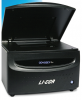
Equipment

Olympus FV1000MP Multiphoton Excitation Fluorescence...

Olympus FV1000MP Multiphoton Excitation Fluorescence Microscope (MPEF) ... also capable of SHG (ex. 840 nm --> 420 nm) ***...

Read More

Li-Cor Odyssey CLx

Li-Cor Odyssey CLx fluorescence scanner. This instrument is hosted by Prof. Donowitz lab and use is intended for G.I. Center...

Read More
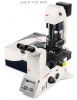
. Leica SP8 confocal microscope

The Leica SP8 confocal microscope is on a Leica DMi8 inverted microscope stand (DMi8CEL).  * open access to JHU (and...

Read More

MetaMorph Key 1 (#34135)

MetaMorph Key 1 is license #34135. Ross 9th floor users: If your preferred Windows PC does not have this license installed,...

Read More
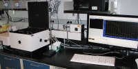
zzzz Retired Perkin-Elmer EnVision Plate Reader

New users can contact George McNamara to coordinate training by PerkinElmer's Matt Reuter & Carl Apgar: George...

Read More